Solar PV Manufacturing Value Chain
Polysilicon, Ingots, Wafers, Cells, Modules
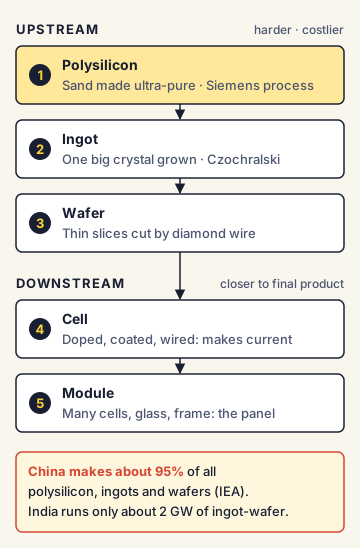
A solar panel is not made in one step. It is made in a chain of five main stages: polysilicon → ingot → wafer → cell → module. Each stage takes the product of the earlier stage and turns it into something more advanced. This whole chain is called the solar PV (photovoltaic) manufacturing value chain. A country that controls the early stages of this chain has great power over everyone who makes panels later.
Why does this chain matter?
Solar power is now the fastest-growing source of electricity in India and the world. But you can only install solar plants if you can get panels. If one country makes almost all the parts, other countries depend on it, just like a town that buys all its rice from one shop. If that shop raises prices or stops selling, the town is in trouble. So the question "who makes each stage?" is a question of energy security, jobs and trade, not just technology.
Stage 1: How is polysilicon made?
The story starts with ordinary sand or quartz, which is mostly silica (silicon dioxide). Quartz is heated with carbon in a very hot electric arc furnace. This gives metallurgical-grade silicon, which is about 98 to 99% pure. That is not pure enough for solar cells. So it is turned into a gas-like chemical called trichlorosilane, cleaned by distillation, and then deposited on hot silicon rods (heated to around 1,100°C) inside a reactor.
This method is called the Siemens process, and it is still the main way polysilicon is made. The result is polysilicon: silicon that is extremely pure. Solar-grade polysilicon is usually at least 99.9999% pure ("six nines"); chips need even purer silicon, about nine nines. This stage uses huge amounts of electricity and needs big, costly plants.
Stage 2 and 3: Ingots and wafers
The polysilicon chunks are melted. A small seed crystal is dipped in and slowly pulled up while rotating. The silicon grows around it as one single, perfect crystal in the shape of a long cylinder. This is called an ingot, and the method is called the Czochralski method. The ingot is then sliced with very fine diamond wires into thin squares called wafers, thinner than a fingernail.
Wafer sizes are named by their side length. Two common sizes today are M10 (182 mm) and G12 (210 mm). Bigger wafers mean more power from each panel.
Stage 4: The solar cell
A wafer by itself does not make electricity. It is treated with small amounts of other elements (this is called doping), given an anti-reflective coating, and printed with thin metal lines that collect current. Now it is a solar cell. When sunlight falls on it, it pushes electrons to move, which creates an electric current. This is the photovoltaic effect. Different cell designs have names such as:
- PERC (Passivated Emitter and Rear Cell): the older mainstream design.
- TOPCon (Tunnel Oxide Passivated Contact): the newer mainstream design, a little more efficient.
- Heterojunction (HJT): combines crystalline silicon with very thin layers of another type of silicon.
Stage 5: The module
Many cells (often 60 to 144, or half-cells) are connected together, placed under strong glass, sealed with a plastic layer and fixed in an aluminium frame with a junction box. This finished product is the solar module, which most people call a solar panel. Module assembly is the easiest and cheapest stage to set up. That is why many countries start here and move "upstream" (towards polysilicon) later.
What comes next: perovskite and tandem cells
Ordinary silicon cells are close to their natural upper limit of efficiency. A single-layer cell can never turn more than about a third of sunlight into electricity (scientists call this the Shockley-Queisser limit, about 33.7%). Perovskites are a family of man-made crystal materials that are very good at absorbing light and can be made cheaply as thin films, almost like printing ink.
When a perovskite layer is placed on top of a silicon cell, each layer catches a different part of sunlight. This is a tandem cell. In April 2025, a perovskite-silicon tandem cell made by the Chinese company LONGi reached a certified efficiency of 34.85%, higher than any single-layer cell can ever reach. Perovskites still have problems: they break down faster with heat and moisture, and many contain small amounts of lead. Whoever solves these problems first and makes them at large scale may lead the next generation of solar power.
Who makes what in the world?
China dominates every stage. According to the International Energy Agency (IEA), China's share is above 80% across all main stages, and close to 95% for polysilicon, ingots and wafers. In 2023, Chinese firms made about 95% of all new investment in wafer capacity and 96% in polysilicon. China built this lead over about 15 years through cheap credit, low-cost power, government support and huge scale. This scale has made solar panels very cheap for the whole world, but it has also created dependence.
India's position (as of October 2026)
India has built module capacity very fast, but the upstream stages are still small:
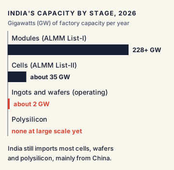
- Modules: over 228 GW of capacity listed by the Ministry of New and Renewable Energy (MNRE) on its approved list (September 2026).
- Cells: about 35 GW listed (August 2026), much smaller than module capacity.
- Ingots and wafers: only about 2 GW actually operating; a pipeline of about 30 GW is planned, but large-scale polysilicon production has not yet begun.
- Installed solar power: about 171 GW (September 2026).
So India makes many modules but still imports most of the cells, wafers and polysilicon, mainly from China. India's main tools to change this are:
- ALMM (Approved List of Models and Manufacturers): an MNRE list from the ALMM Order, 2019. Government-linked and many other projects must use only listed products. List-I covers modules. List-II, for cells, became mandatory from 1 June 2026. A List-III for wafers has been proposed from 1 June 2028.
- PLI Scheme for high-efficiency solar modules: cash rewards for producing in India, with extra weight for factories that make more of the chain (explained in the next bridge).
- Basic Customs Duty (BCD): import taxes on foreign cells and modules (in force since April 2022, restructured in the 2025-26 Budget) to make domestic products more competitive.
Commonly confused concepts
- Cell vs module: A cell is one single unit made from one wafer. A module is many cells joined, framed and sealed. You install modules, not single cells.
- Polysilicon vs ingot vs wafer: Polysilicon is the purified raw material in chunks. An ingot is a large single block grown from melted polysilicon. A wafer is a thin slice cut from the ingot.
- Upstream vs downstream: Upstream stages (polysilicon, ingot, wafer) are closer to the raw material, harder and costlier. Downstream stages (cell, module) are closer to the final product.
- Module capacity vs installed capacity: Module manufacturing capacity is how many GW of panels factories can make each year. Installed capacity is how many GW of solar plants are actually running.
- Solar PV vs solar thermal: PV turns sunlight directly into electricity. Solar thermal uses sunlight to make heat (for water heaters or to make steam that runs a turbine).
Issues, criticism and the way forward
- Upstream dependence: India's module capacity looks large, but without its own polysilicon and wafers it still depends on imports for the hardest parts.
- Technology gap: The machines and know-how for advanced cells and wafers mostly come from China. Controls on technology exports can slow India's upstream plans.
- Cost: Indian-made modules and cells often cost more than Chinese ones. Rules like ALMM and import duties protect local factories but can raise costs for solar developers and, in the end, for electricity buyers.
- Unused capacity and quality: Some listed module capacity uses older technology or runs below full use. Quality testing needs to keep up.
- Power and water needs: Polysilicon plants need cheap, steady power and lots of water, which are not easy to get everywhere.
- Way forward: experts suggest stable long-term policy (ALMM phases, PLI), cheaper finance for upstream plants, research on next-generation cells such as perovskites and tandems, recycling of old panels to recover silicon and silver, and partnerships with trusted countries for machines and know-how.
Concepts to Know
- Photovoltaic (PV): "Photo" means light and "voltaic" means electricity. PV technology turns light directly into electricity.
- GW (gigawatt): A unit of power. 1 GW = 1,000 MW (megawatts). 1 GW of solar panels is roughly enough, at peak sunshine, to power several lakh homes.
- Efficiency (of a solar cell): The share of sunlight falling on the cell that it turns into electricity. A 22% efficient cell turns 22 units of sunlight energy out of 100 into electricity.
- Doping: Adding a tiny amount of another element (like boron or phosphorus) to silicon to change how electricity flows through it. This is what lets a cell create a current.
- Diamond wire: A very thin steel wire coated with diamond dust, used like a saw to cut ingots into wafers with little waste.
- Value chain: All the steps a product goes through from raw material to finished good, with each step adding value.
- Five stages: polysilicon → ingot → wafer → cell → module
- Siemens process: main method for making high-purity polysilicon; Czochralski method: grows single-crystal ingots
- Common wafer sizes: M10 = 182 mm, G12 = 210 mm
- Single-junction cell efficiency limit (Shockley-Queisser): about 33.7%; record perovskite-silicon tandem: 34.85% (LONGi, April 2025)
- China's share: over 80% across main stages; about 95% in polysilicon, ingots and wafers (IEA)
- India (2026): over 228 GW module capacity on ALMM List-I (September); about 35 GW cells on List-II (August); about 2 GW ingot-wafer operating; about 171 GW solar installed
- ALMM Order, 2019 (MNRE); List-II (cells) mandatory from 1 June 2026; List-III (wafers) proposed from 1 June 2028
● Tracked since August 07, 2026 · last seen October 18, 2026 · updates as the daily brief publishes